SiDBI Uses Silicon Technology to Package Unique LEDs
2011/05/24 | By Ken LiuThe silicon-backed packaging approach features prime advantage of efficient thermal conductivity
Silicon Base Development Inc. (SiBDI) uses a unique packaging method for its light-emitting diodes (LEDs), involving the fixing of an LED epitaxy layer onto a flexible copper-alloy sheet that is, in turn, fixed to a 200mm silicon wafer.

The LED packager, based in Taoyuan, Taiwan, has borrowed this method from silicon-chip manufacturing thanks to the widespread silicon-chip experience of its management. “Our chairman, Mark Tuttle, is the former chief technology officer for DRAM chipmaker Micron Technology,” explains, Simon Hsu, special assistant to the company's general manager. Both Micron and SiBDI, he notes, belong to an Iowa-based holding company.
The prime advantage of the silicon-backed packaging approach is efficient thermal conductivity. “The silicon-based approach limits the thermal resistance of a high-power package to within 5 degrees Celsius per watt,” Hsu says. “I'm talking about a single-chip package, not multi-chips or a chip-array package.” Thermal conductivity, he adds, is trickier with a single-chip high-power package than with the others.
Hsu's information indicates that copper alloy conducts heat at a rate of 400 W/mK while for silicon the figure is 150 W/mK. Both materials are crucial to microchip manufacturing, which etch copper layers onto micron-grade circuits on silicon wafers to conduct electricity.
The silicon approach offers an ideal solution not only for heat dissipation but also for the connection of circuits on different substrate layers in a package. The company employs through-hole or deep-etching technology, which is commonly used to connect the circuits on different substrate layers of a logic IC package. “MEMS [micro-electro-mechanical] technology is far more than enough for LED packaging, as it usually handles over 10 substrate layers in an IC chip package while an LED package has only two layers,” Hsu explains.

The company includes high-power chips made by SemiLEDS, headquartered in Iowa and reportedly the world's No. 2 supplier of high-power chips by volume. The firm's I-Do chip gives off 135 lumens at 351mA, and it is known for vertical-structure chips whose top and bottom ends serve as anodes and cathodes; this allows a freer flow of electrical current than is possible with horizontal-structure, whose anodes and cathodes are narrow strips on the sides. “The result,” Hsu says, “is that more heat builds up on horizontal chips.”
Sidestepping Patent Woes
This unique LED packaging technology, Hsu stresses, frees his company from patent disputes. Copper alloy is crucial to SiDBI's packaging approach, not only because of its superb heat conductivity but also because of its uniqueness in relation to other existing methodologies. “There is some difference between the alloy for LED packaging and the alloy for DRAMS,” Hsu explains. “Our LED packages require a double-digit-micron layer, whereas DRAM chips need only single-digit micron layers, and our LED packages require a thicker layer because the major purposes of the layer are thermal conductivity and impact resistance.”
Some new entrants into the field grow epitaxy layers directly on silicon wafers in a bid to escape patent issues, but Hsu claims that this approach, compared with other silicon-based approaches, assures only lower efficiency in converting electrons into photons. “Basically,” he says, “our layers are grown on sapphire and are removed from the substrate for mounting on copper ally. So we haven't had that problem.”

Hsu is optimistic about SiDBI's prospects, saying that the company has many advantages over its larger rivals. “We are absolutely not the forerunner in the lumens-per-watt competition,” he concedes, “but we're confident that the cost of each lumen that our products generate is lower than that of the big players.”
The products are competitive even with rival products made of arrays of low-power chips, Hsu insists: “A typical multichip package for a backlight sells for NT$1.2 per 6 lumens; our 220-lumen product, at 700mA, goes for NT$30—roughly NT$1 per 7.3 lumens.”
In-house production of silicon substrates further strengthens the company's grip on quality and cost.
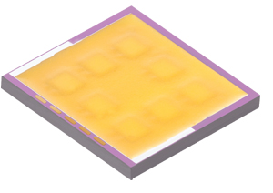
SiDBI is superior to the big players in thermal performance and tailor-made services, Hsu believes. “Our typical 7.9mm x 7.9mm LED module can carry eight SemiLED chips,” he explains. “Cree-made modules [Cree is the world's No. 1 supplier of high-power LED chips] of this size can hold only four high-power chips.”
In March this year SiDBI acquired Taiwan's Helios Crew Corp., a packaging materials company, and its packaging materials, lead-frame packaging, and phosphor know-how make SiDBI stronger than ever. As Hsu sums it up, “We now have SemiLED chips, knowledge about packaging materials, and silicon-based technology. All of these constitute a solid foundation for competitiveness.”


